Final Schematic of CMOS XNOR Explained | Step-by-Step CMOS Design | VLSI Schematic Tutorial (Part-2)
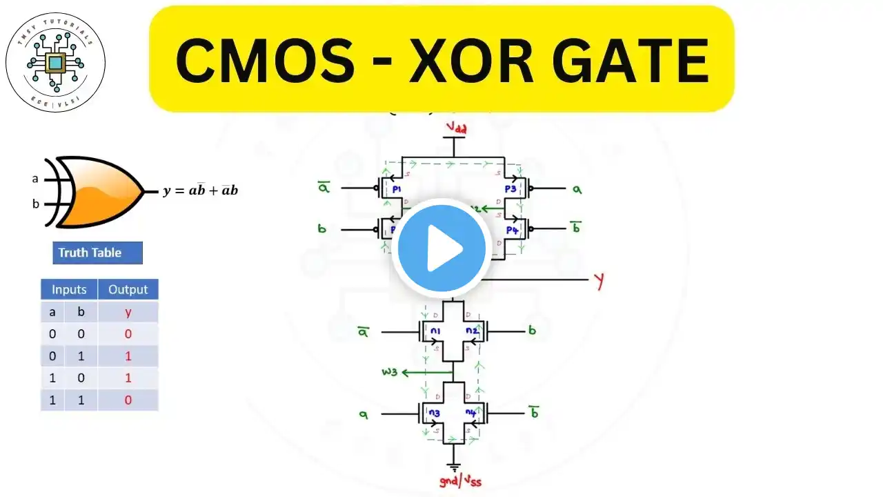
Description: In this video, we present the Final Schematic of CMOS XNOR Gate — the second part of our CMOS XNOR Design Series. This tutorial takes you through the complete transistor-level design of the CMOS XNOR circuit, focusing on the practical schematic creation process using Cadence Virtuoso and other EDA tools. The CMOS XNOR gate is one of the most fundamental building blocks in digital design, widely used in comparators, parity generators, adders, and arithmetic circuits. Understanding how to design and implement it at the transistor level helps VLSI students and professionals gain deeper insight into logic design, switching characteristics, and timing behavior of digital circuits. 🧠 Introduction to CMOS XNOR Design The CMOS XNOR circuit combines PMOS and NMOS transistors in a complementary structure to realize the Boolean function: Y = (A ⊙ B) = A’B’ + AB This circuit requires 8 to 10 transistors for efficient implementation, balancing speed, power, and area trade-offs. In this Part-2 video, we focus on the final schematic design, connecting transistor networks properly to generate accurate logic functionality. ⚙️ What You’ll Learn in This Video How to connect Pull-Up (PMOS) and Pull-Down (NMOS) networks for XNOR implementation. Step-by-step schematic design using Cadence Virtuoso or similar EDA tools. Logical verification and connectivity checks for the final CMOS XNOR schematic. Design challenges: transistor stacking, sizing, and symmetry for noise margin balance. Impact of design on propagation delay, power dissipation, and timing closure in synthesis and STA. Importance of CMOS XNOR in arithmetic circuits, data comparators, and logic equivalence checking. 🧾 Topics Covered ✅ Boolean Expression of XNOR ✅ CMOS Implementation Logic ✅ Pull-Up and Pull-Down Network Construction ✅ Transistor-Level Schematic in Cadence ✅ Signal Flow and Output Verification ✅ Design Challenges and Common Mistakes ✅ Practical Application of XNOR in VLSI Design 💡 Why This Topic Matters Understanding CMOS XNOR schematic design builds a strong foundation in custom digital circuit design, crucial for anyone aiming to work in VLSI front-end or back-end domains. Whether you’re preparing for VLSI interviews, learning circuit design fundamentals, or exploring custom cell creation, mastering this schematic is essential for understanding transistor-level logic synthesis and timing path optimization. 🎯 Call to Action: Watch the full video till the end to clearly understand how the Final CMOS XNOR Schematic is designed and verified. Don’t forget to Like, Share, and Subscribe to TMSY Tutorials for more VLSI, Digital Design, and EDA Tool-based Tutorials! Your support helps us create more content on Standard Cell Design, Characterization, Synthesis, and STA. #Hashtags: #cmosxnor #vlsidesign #edatools #cmoslogicgates #vlsitutorials #tmsytutorials #cmoscircuitdesign #digitallogicdesign #cadencevirtuoso #synopsys #vlsi #synthesis #sta #cmosxnorimplementation #standardcelldesign #vlsistudents #vlsiprojects #vlsitraining #madeeasyfaculty #vlsiindia #vlsicourses ✨ Hashtags for reach: #tmsytutorials #tmaharshisanandyadav #statictiminganalysis #sta #DTA #vlsi #vlsitraining #chipdesign #synthesis #physicaldesign #PrimeTime #tempus #redhawk #STAtools #DTAtools #STAinVLSI #DTAinVLSI #TimingAnalysis #timingclosure #VLSITutorials #VLSILearning #VLSIInterviewQuestions #VLSICourse #vlsijobs #asic #fpga #vlsidesign #rtldesign #RTLtoGDSII #digitaldesign #Voltus #cadence #synopsys #ansys #designcompiler #genus #Innovus #edatools #socdesign #chipverification #staticanalysis #dynamicanalysis #TimingVerification #STAflow #STAprocess #TimingReports #DelayCalculation #SetupTime #HoldTime #clocktreesynthesis #cts #signalintegrity #PowerAnalysis #IRDrop #EMAnalysis #NoiseAnalysis #GateLevelSimulation #PostLayoutSimulation #FunctionalVerification #RTLVerification #TimingSignoff #SignoffTools #STAengineer #DTAengineer #BackendDesign #frontenddesign #ChipImplementation #asicdesign #FPGAprototyping #icdesign #semiconductors #SiliconDesign #vlsiprojects #VLSIResearch #StandardCells #LibraryCharacterization #eda #hardwaredesign #logicdesign #circuitdesign #digitalelectronics #edasoftware #ChipTapeout #VLSILab #VLSItools #NetlistAnalysis #SDF #LibFiles #SDFAnnotation #TimingLib #TimingClosureFlow #designflow #RTL2GDS #EDAflow #SemiconductorEngineering #SoCtiming #AdvancedNodes #TimingOptimization #ClockDomainCrossing #VLSItips #ece #engineering #osmaniauniversity 📚 Watch More VLSI Tutorials: YouTube: / @maharshisanandyadav Udemy: https://www.udemy.com/course/digital-... Instagram: / vlsi.tmsy.tutorials LinkedIn: / t-maharshi-sanand-yadav